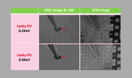
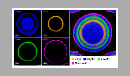
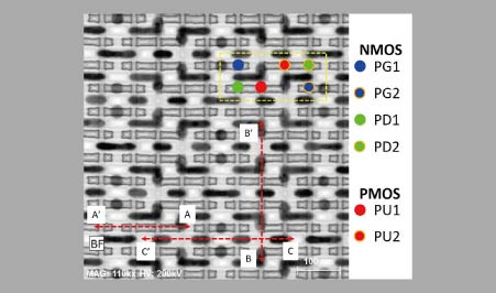
Technology innovations 25c-2: A closer look at Samsung 3nm GAA transistors
 2025.4.17
 TECHNOLOGY INNOVATIONS

...
Technology innovations 25c-1: High-resolution chemical composition analysis for advanced process - EELS analysis
2025.3.26
TECHNOLOGY INNOVATIONS
...
.png)
Feedbacks from key clients in US and Europe
2024.10.9
TECHNOLOGY INNOVATIONS
We have been receiving quality professional services on semiconductor materials analysis, including ...
TEM analysis on Samsung 5 nm technology node
2018.4.17
TECHNOLOGY INNOVATIONS
TEM with high spacial resolution has been widely utilized to analyze advanced chips. The sample is S...
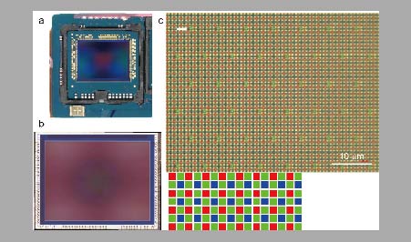
Materials and surface analyses on Samsung image sensor
2018.4.17
TECHNOLOGY INNOVATIONS
Materials and surface analyses are utilized to unveil inner structures of the Samsung image sensor. ...
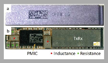
Analysis on Qualcomm 5G mmWAVE AiP
2018.4.17
TECHNOLOGY INNOVATIONS
OM image of Qualcomm 5G mmWAVE AiP, QT525 AiP purchased from the market is shown in a. After removin...
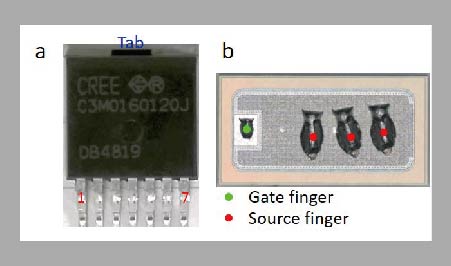
Materials analysis on SiC MOSFET
2024.10.9
TECHNOLOGY INNOVATIONS
It has been proved that SiC MOSFET has much greater efficiency compared to Si version, especially at...
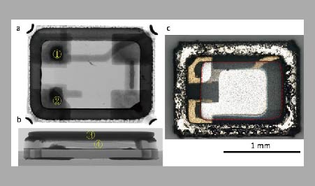
PFIB analysis on quartz device
2024.10.9
TECHNOLOGY INNOVATIONS
Quartz device is a common component in all electronic products from EV, 5G, IoT, aerospace, and AI. ...
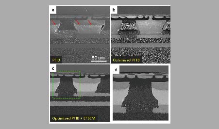
MSS niche analysis on substrates: PFIB and advanced imaging method
2024.10.9
TECHNOLOGY INNOVATIONS
Preparing cross-sectional substrates by Ga FIBs is time-consuming due to their lateral size. ...
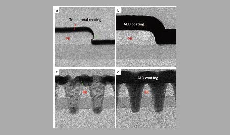
Low-temperature ALD application for photoresists
2024.10.9
TECHNOLOGY INNOVATIONS
Photoresist (PR), a commonly used materials in IC lithography, is extremely sensitive to temperature...
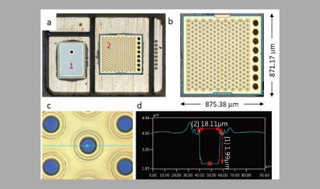
Materials analysis on VCSEL
2024.10.9
TECHNOLOGY INNOVATIONS
Materials analysis on a VCSEL (Vertical-cavity surface-emitting laser) chip, purchased from the mark...
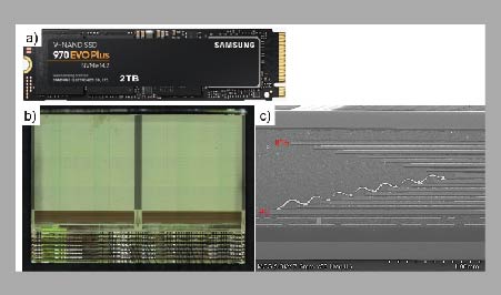
Materials analysis on 3D V-NAND
2024.10.9
TECHNOLOGY INNOVATIONS
NAND flash memory, a type of non-volatile storage memory, can be found everywhere in our daily life,...