 TECHNOLOGY INNOVATIONS
TEM with high spacial resolution has been widely utilized to analyze advanced chips.
The sample is Samsung cellphone’s AP, purchased from the market, and the chip is fabricated by Samsung 5 nm technology.
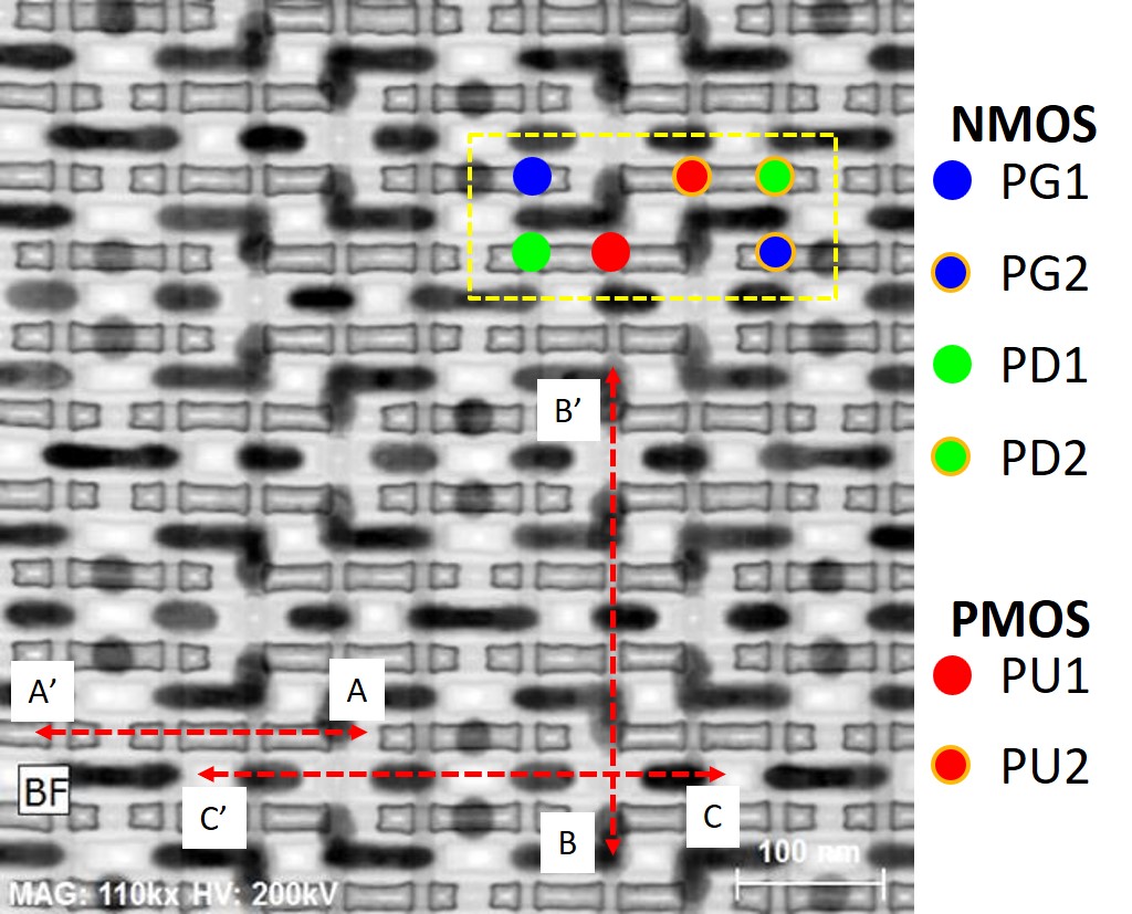
The target of interest for TEM analysis is 6T SRAM.
This image shows PV TEM result of 5 nm technology node 6T SRAM.
One 6T SRAM cell is composed of four NMOSs and two PMOSs, and one of cells is outlined by the yellow-dotted rectangle, where individual transistor is marked by circles with different colors.
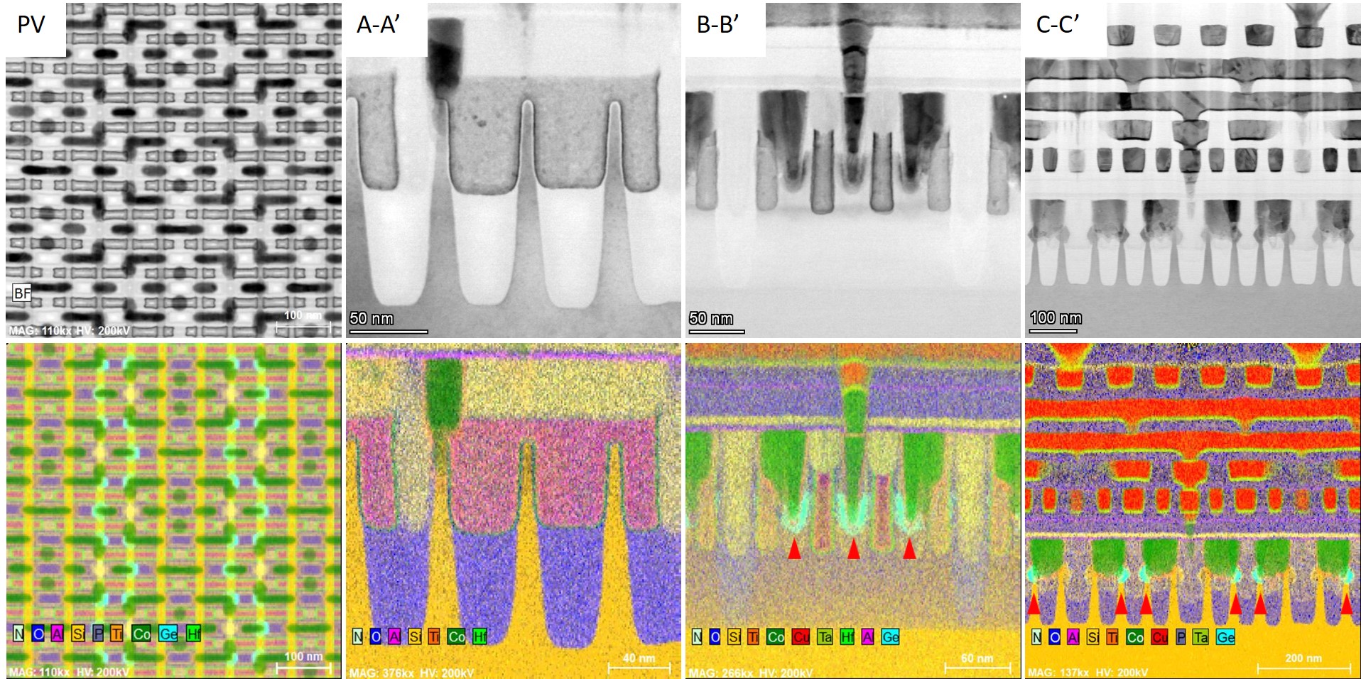
PV TEM image together with three cross-sectional TEM (XTEM) images of 5 nm technology node 6T SRAM cut along with A’A (on gate), B’B (along P-fin), and C’C (on SiGe & SiP), respectively.
The cut directions are exhibited in the previous image.
Their EDS mapping are shown in the lower column, accordingly.
For easy identification, SiGe are marked by the red triangles.
| Application process | Exynos 7420 14 nm node |
Exynos 8895 10 nm node |
Exynos 9630 8 nm node |
Exynos 2100 5 nm node |
|---|---|---|---|---|
| Length (nm) | 467.1 | 382.2 | 384.9 | 244.9 |
| Width (nm) | 168.8 | 129.9 | 126.5 | 110.2 |
| Area (nm2) | 78,846 | 49,648 | 48,672 | 26,975 |
| Fin height (nm) | 42.0 | 48.6 | 51.6 | 54.6 |
| Fin width (nm) | 8.5 | 5.9 | 5.6 | 8.2 |
| Fin pitch (nm) | 177.6 | 136.5 | 136.4 | 72.9 |
| Gate width (nm) | 33.4 | 22.5 | 19.7 | 18.0 |
Critical dimension (CD) comparisons among different technology nodes (14 nm, 10 nm, 8 nm, and 5 nm) from Samsung fabrication technology.
Please note the umbers shown in this table are acquired by MSS TEM/STEM results taken only at 6T SRAM areas.