2D 3D X-ray
▍3D X-ray
- ★reselotion down to 500nm
- • Non-destructive sub-micron scale microscopy of intact samples
- • Higher flux and faster scans without compromising resolution
- • True spatial resolution of 500 nm with a minimum achievable voxel size of 40 nm
- • High resolution across a broad range of sample types, sizes, and working distances
- • In situ imaging for non-destructive characterization of microstructures in controlled environments and over time
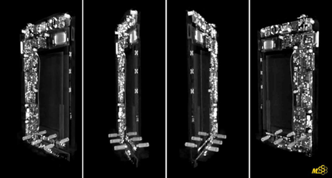
▍Asus Zenfone 3D X-ray results

▍Eng. Contact Window
Mr. Wu ext.3010
E-mail: nde@msscorps.com
The X-Ray has very short wave length and high electromagnetic radiation.
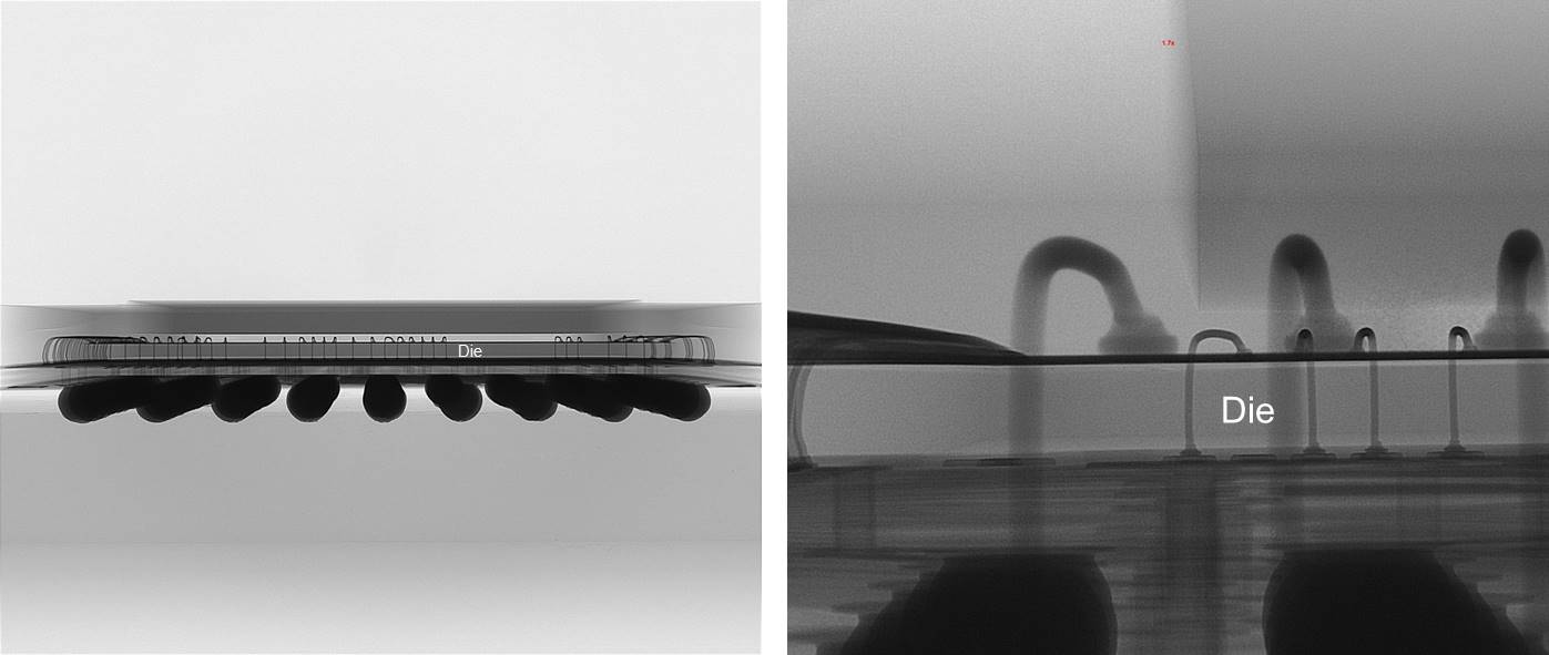
When the sample location cannot be inspected using external appearance related metrology tools, X-Ray imaging can be used to detect the internal structure of the sample due to its intensity change as a function of material density. This contrast image can show the internal structure of the sample without any physical destruction to the diagnosed region.
▍Equipment
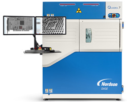
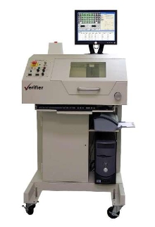
MSS has the newest X-ray equipmet — QUADRA 7 (Nordson DAGE) and FSX-90.
Figure-1. QUADRA 7

Figure-2. FSX-90

▍Specification
- • Sample size:45X40X10(CM)/10kg
- • Power:30~160(KV)
- • Maximum inclination is 70 degrees, 360 degrees rotation
- • Resolution up to 0.1um
- • Machine for real-time observation of images
▍Applications
- • Defect inspection in IC packaging﹕ layer delamination, burst Crack, void, and bonding inspection.
- • Potential defects in the PCB manufacturing process e.g.: mis-alignment, bridge or open circuit.
- • SMT solding void inspection and measurement.
- • Inspection of crack in high density plastic material or void in metal.
- • Solder ball array inspection in BGA packaging and flip chip packaging.
▍Case Sharing
- • Wire&pad burn out
- • 1ST and 2nd bond lift

- •Wire bonding observation

- • Bump adhesion interface inspection
- • Mobile phone internal components inspection
- • Crack
- • front-side
- • L/F bridge
▍Eng. Contact Window
Mr. Wu ext.3010
E-mail: nde@msscorps.com