AFM
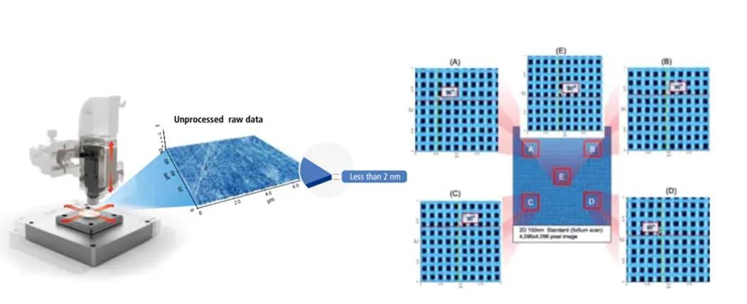
▍NEW! Park NX20
- • Non-destructive & non-contact analysis
- • Maximum sample size–12" wafer
- • High quality analysis result
- • Better spatial resolution,50 Å
- • The appearance size of the sample can be measured
- • 3D shapes can be captured
- • Surface roughness can be quantified as numeric data
- • Decoupled XY and Z scanner, unprocessed row data, & highly linear and orthogonal XY scan


▍Atomic Force Microscopy(AFM)
Atomic force microscopy (AFM) use a special small probe to measure certain interactions between the probe and the sample surface, such as tunneling current, atomic force, magnetic, electromagnetic near field, etc., and use one having a three-axis piezo on the sample surface to scan the sample surface. While scanning ,the vertical axis piezo is able to fine-tune the feedback circuit, so that interaction between the probe and the sample is maintained fixed during the scanning process. The distance between the probe tip and the surface is in a few to several hundred a ° (10-10m) , as long as the recording of the vertical distance, we are able to obtain an image map, these data can be used to show the sample surface characteristic. Most of AFM probes made from the silicon, the tip radius of curvature of about 10nm, is an important research tool for microscopic surface structure.
▍Conductive Atomic Force Microscopy (CAFM)
Conductive Atomic Force Microscopy (CAFM) is to add a set of current amplifier into the AFM microscope, then using Contact Mode to scan the test sample surface, while obtaining the height of the signal, if the sample surface can create current, the probe will also get the current signal. Using CAFM to obtain the height and current distribution of sample surface, and we can compare and identify the location of electrical abnormalities and also can get the current / voltage curve (IV curve) further on a specific point.
▍Equipment
Figure. VEECO INNOVA SPM (Atomic force)
.jpg)
▍Specification
XY > 90um, Z > 7.5umOpen-Loop scanner: XY > 5um, Z > 1.5um
Sample size: X-45mm x Y-45mm x Z-18mm
Motorized Z Axis stage: Z Travel:18mm
Resolution: <2um with standard 10x objective
▍Applications of AFM
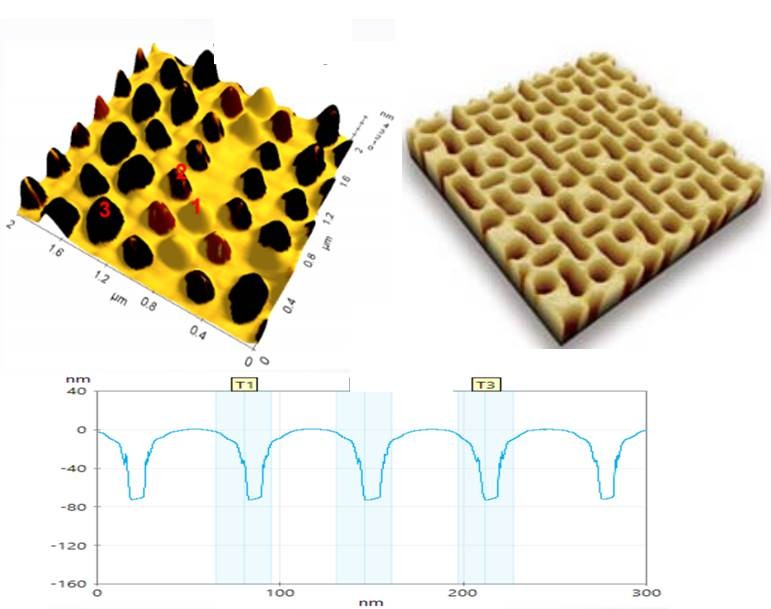
1. Material surface topography
.jpg)
Data storage device surface topography
.jpg)
LED surface topography
▍Applications of CAFM
1.Failure localization (Higher resistance/Junction leakage/Gate oxide leakage)
2.Identify Contact types (P+/N+/Poly contact)
3.I/V curves measurement
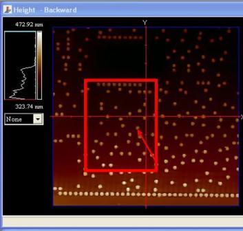
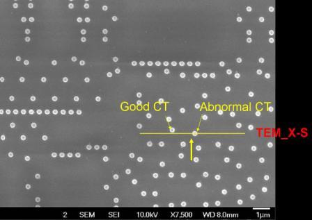
Case 1: Failure localization by CAFM,current map identify the abnormal poly
Case 2 : Failure localization by CAFM,compare the topography and current map
.jpg)
current map

topography
TEM sample preparation after CFAM failure localization

▍Eng. Contact Window
Ms.Huang ext.6218
E-mail: huini_huang@msscorps.com