TEM/EDS
● TEM quality is competitive worldwide
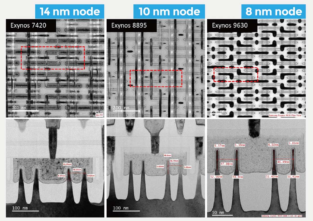
● 5nm FinFET is available
● 2-3 working-day to provide TEM report (sample arrvied)
HOT! FEI Talos, OSIRIS/TEM + JOEL TEM
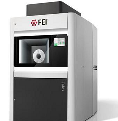
● FEI Talos
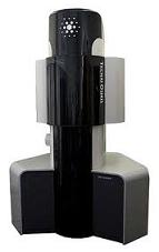
● FEI OSIRIS
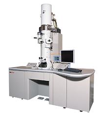
● JEOL 2100F
▍TEM images of Samsung application processes
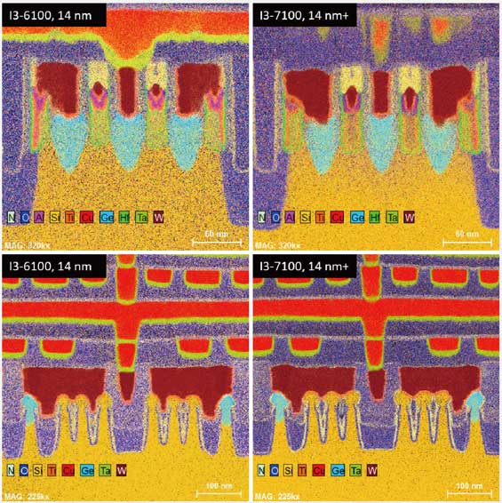
▍EDS mapping of intel CUPs
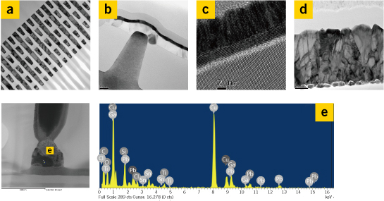
Microstructure analysis: lattice image, IC process monitor, crystal defect observation. Phase identification and composition analysis.
- a TEM inspection of the multi-metal-layer process with Cu dual-damascene structure
- b IC structure observation
- c High resolution TEM with the atomic scale resolution
- d Grain size distribution measurement
- e TEM/EDS analysis for study of Sn whisker growth, the composition distribution of Sn whisker.
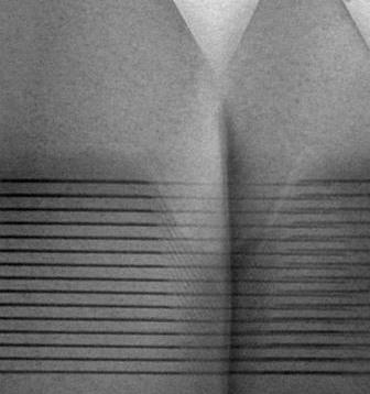
TEM inspection of LED MQWs and dislocation distribution.
▍Eng. Contact Window
mike_chen@msscorps.com