 TECHNOLOGY INNOVATIONS
Materials and surface analyses are utilized to unveil inner structures of the Samsung image sensor.
a & b are OM images of the Samsung image sensor, Samsung S5KGW2 BSI image sensor.
The image sensor is dismounted directly from a Samsung cellphone, purchased from the market.
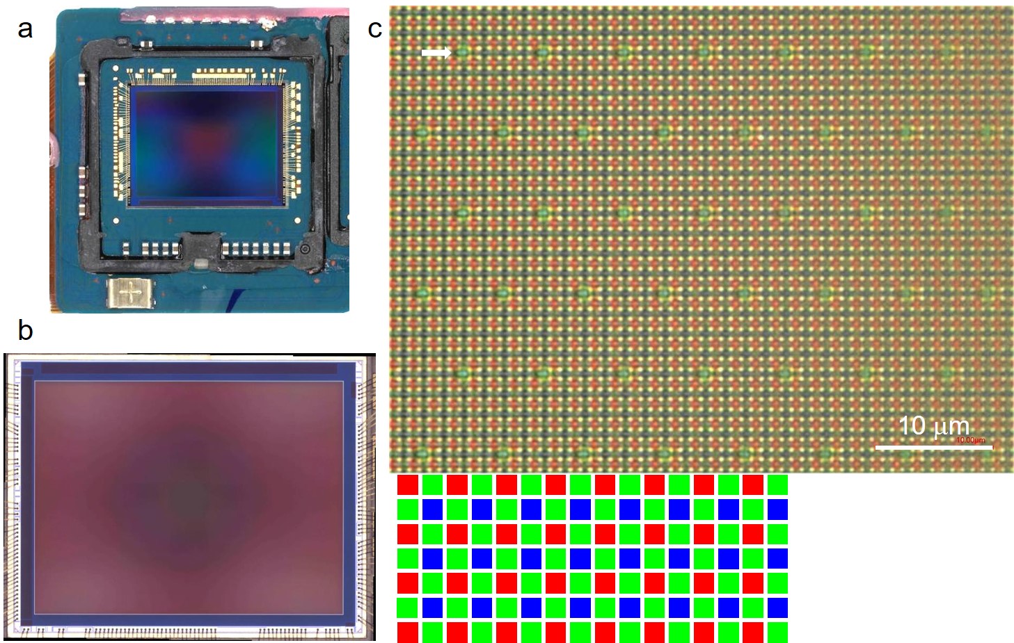
c shows high magnification 3D OM image at the center of the image sensor, clearly exhibits the RGB pixels arrangement.
Besides pixels with normal size, pixels with a bigger size, called super PDs, are also observed in this image sensor.
A super PD, a bigger green cell (G), is marked by the white arrow.
The cartoon below c exhibits RGB cell arrangement in the image sensor.
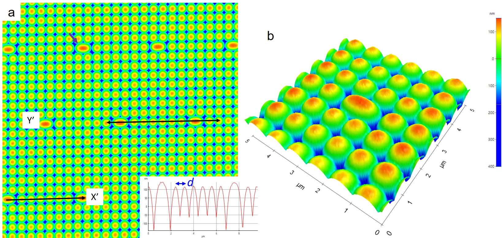
To unveil the surface morphology of the image sensor, microlens (ML), AFM is utilized as shown in a and the line profile along the black double arrow shown in the inset of a suggests the interspacing of the ML cell, d, is 0.8 m. A super PD is marked by the purple arrow.
3D perspective of the ML, image reconstruction based on the AFM data, is shown in b to clearly exhibit the appearance of the ML cell.
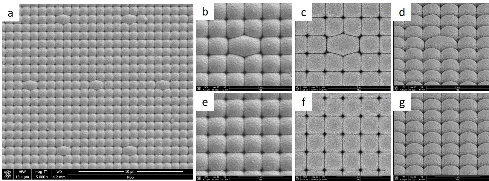
For Materials analysis on the Samsung image sensor, we start with SEM to image the surface of the ML cells.
a is the top-view SEM image of the ML cells.
b-d and e-g are higher magnification SEM images of the ML cells taken with different imaging modes and viewpoints (tilted view).
Detailed structural information of the ML cell can be clearly resolved with different imaging modes.
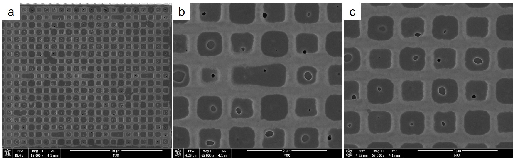
a-c are SEM images of the Grid structure taken with different magnifications.
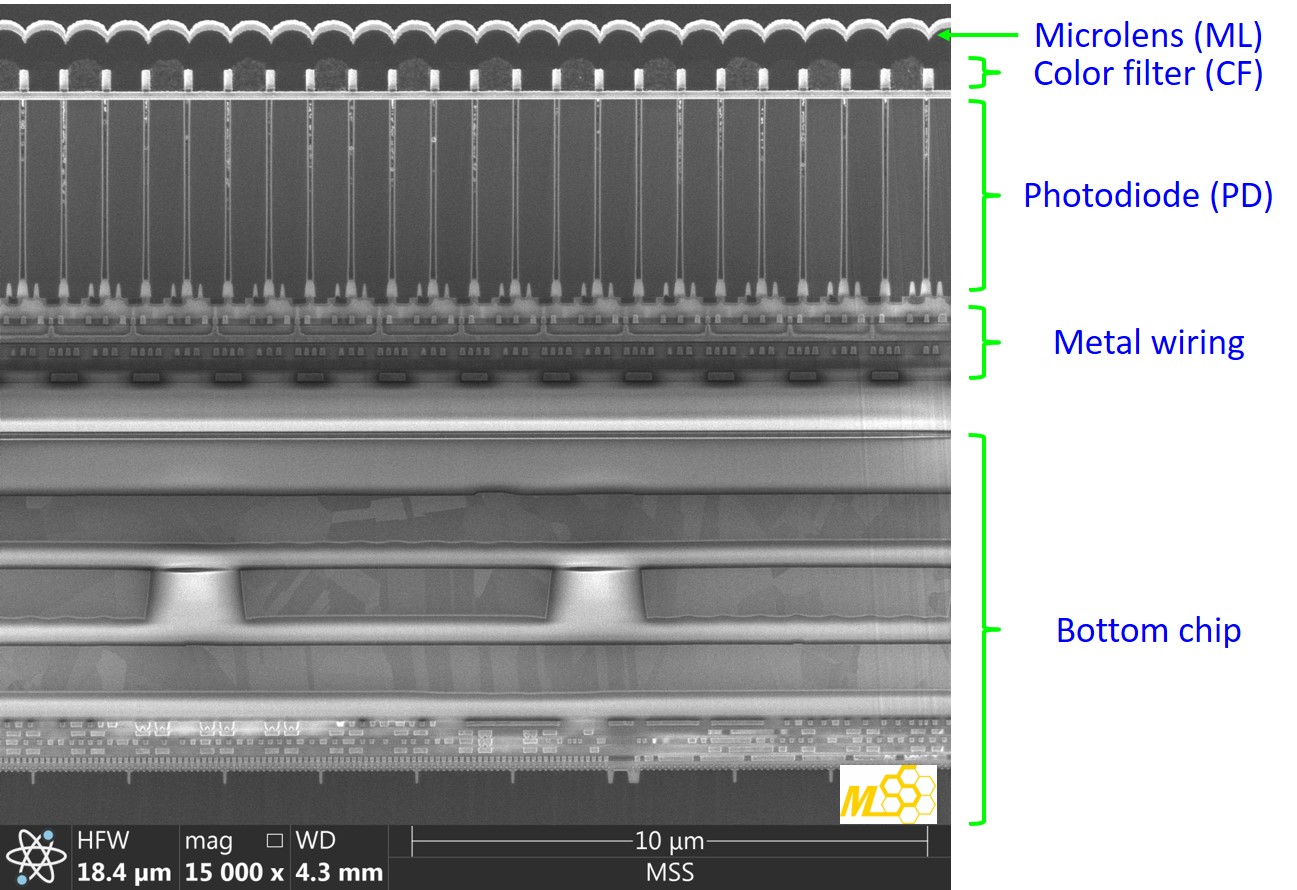
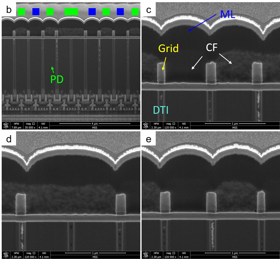
To understand the inner structures of the Samsung image sensor, cross-sectional SEM is utilized.
a shows cross-sectional overview SEM image of the image sensor, where each layer structure is identified.
The details of the inner structures, such as PD, ML, DTI, and CF, can be clearly resolved with higher magnification cross-sectional SEM images as shown in b-e.
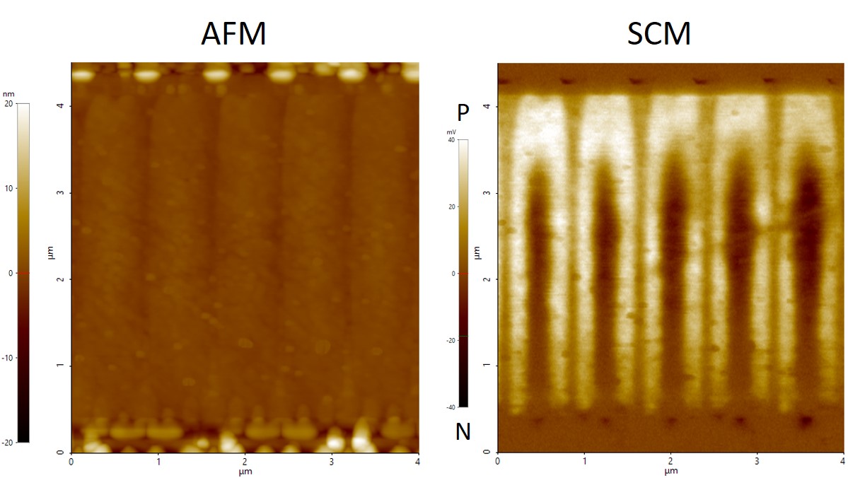
To unveil the PN structure of the PD, SCM, one of powerful tools of surface analysis, is utilized.
Firstly, a cross-sectional sample at the PD center is prepared.
a shows cross-sectional AFM morphology of the image sensor.
No clear structures (featureless) in the PD can be observed, suggesting the PD surface is very flat.
When we switch to SCM analysis, clear PN structure in the PD center can be observed as shown in b.
Our materials and surfaces analyses provide important structural and electronic information of the image sensor.