 TECHNOLOGY INNOVATIONS

OM image of Qualcomm 5G mmWAVE AiP, QT525 AiP purchased from the market is shown in a.
After removing the outer shell, b, the inner components can be seen, including PMIC, TxRx, inductance, and resistances.
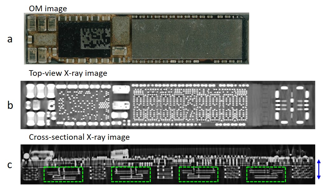
The first step of the analysis on Qualcomm 5G mmWAVE AiP is non-destructive , including OM and X-ray analyses.
OM image, top-view X-ray image, and cross-sectional X-ray image are shown in a, b, and c, respectively.
In c, mmWAVE antennas, marked by the green-dotted rectangles, can be clearly observed.
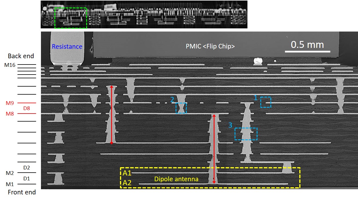
The upper shows the cross-sectional 3D X-ray image of Qualcomm 5G mmWAVE AiP.
The lower is the cross-sectional SEM image analyzed at the location marked by the green-dotted rectangle in the upper image.
This image exhibits all detailed inner structures of Qualcomm 5G mmWAVE AiP.
The dipole mmWAVE antenna is at M1-D1-M2 and the substrate core is at M8-D8-M9.
Note: M represents metal layer and D represents dielectric layer.
Current flow in different metal layers is achieved via the vertical metal lines, two of them are indicated by the red-double arrows.
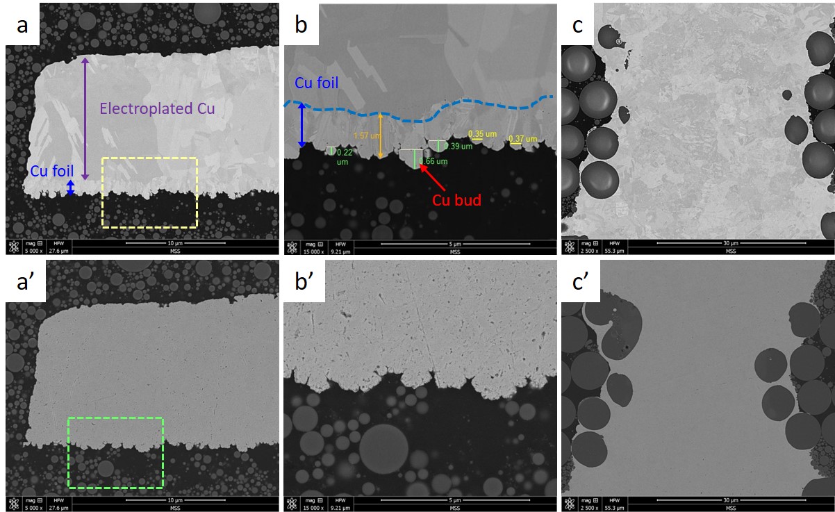
In order to unveil the details of the metal layers in Qualcomm 5G mmWAVE AiP, SEM is utilized.
a shows a higher magnification SEM image of the metal layers taken at the locations marked 1 in the previous image.
b & c are further zoom-in SEM images at the location marked by the yellow dotted rectangle in a.
To lower signal loss and have a better transmission quality especially at higher frequency, it is crucial to understand the detailed structures at the edge of the metal layers, such as Cu buds.
With the help of MSS advanced imaging method, structures of the Cu foil and Cu buds can be obtained, as shown in a-c.
Images acquired with the normal method are shown in a’-c’ for comparison. No clear inner structures can be observed.