 TECHNOLOGY INNOVATIONS
It has been proved that SiC MOSFET has much greater efficiency compared to Si version, especially at higher voltage.
Here, we would like to use our niche materials analysis to unveil the detailed structure of a SiC MOSFET.
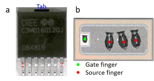
The SiC MOSFET we use is Cree SiC power n-MOSFET, purchased from the market and its OM image is shown in a.
In total, there are 7 pins, from 1 to 7, where pin 1 is Gate, pin 2 is Driver source, and pins 3-7 are Power source.
b is a OM image of the SiC MOSFET after decapsulation.
Three Source fingers are found suggesting this SiC MOSFET is capable of carrying higher current.
To unveil the inner structures of the SiC MOSFET, cross-sectional SEM analysis is utilized.
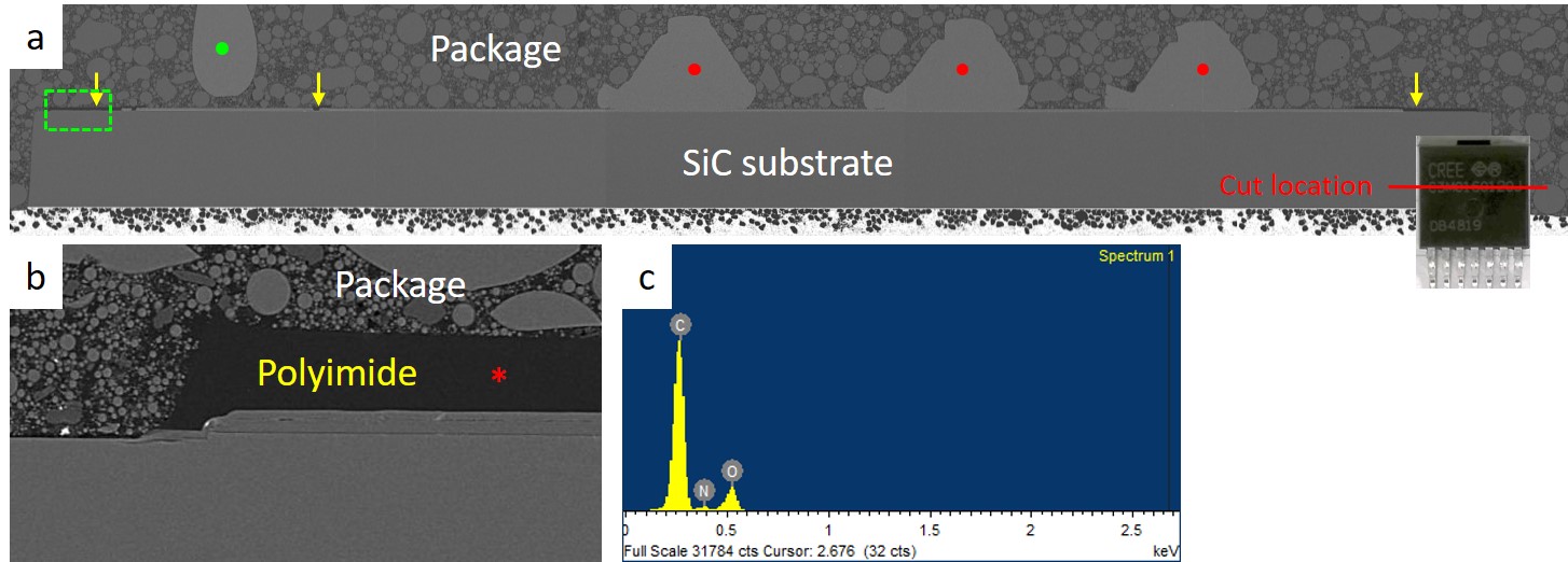
a is an overview SEM image of the SiC MOSFET.
The cutting location is marked by the horizontal red line in the inset of a.
Zoom-in SEM image in the location marked by the green-rotted rectangle is shown in b.
From the image, it clearly shows that there is one polyimide layer on part of the SiC MOSFET surface.
Such design is believed due to the high voltage protection considerations.
EDS analysis is then utilized on the polyimide layer, marked by the red *, to understand its chemical composition.
The point EDS results are shown in c, where three main elements can be detected, C, O, and N.
It is extremely important to have low-resistance ohmic contacts to realize high-performance SiC MOSFET.
There are two ways to reduce the ohmic contact resistance, either reduction of the barrier height at metal/SiC interface or increase in the doping concentration in the SiC substrates.
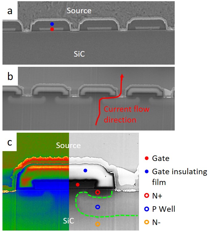
Here, we would like to demonstrate one of MSS niche analyses to unveil the doping distribution of the SiC MOSFET by SEM.
With the help of MSS advanced imaging method, doping distribution can be clearly seen as shown in b.
Images acquired with the normal method are shown in a for comparison.
No clear doping distribution can be observed.
The red arrow in b exhibits the current flow when the chip is ON.
With the help of the color scale rendering, fine structures of the SiC MOSFET can be seen in the further zoom-in SEM image, c.
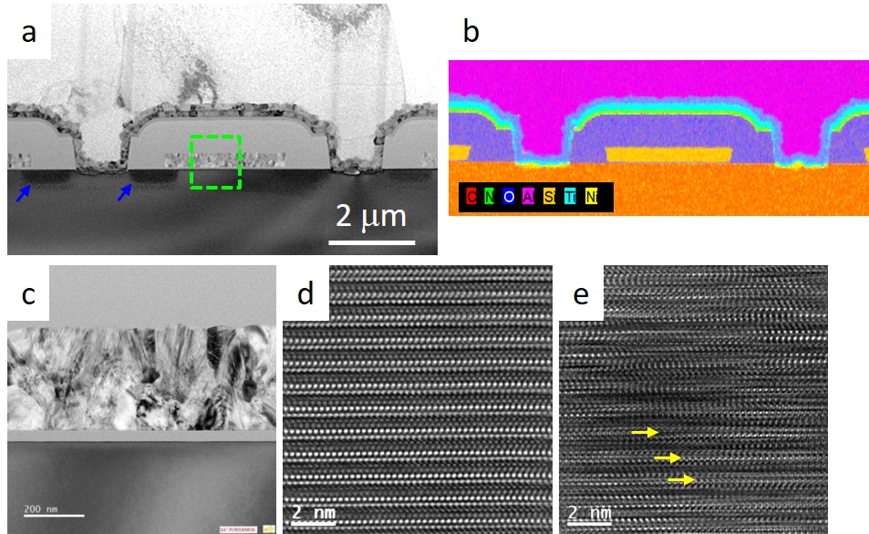
Besides SEM, TEM with high spatial resolution is also utilized.
a is a TEM image of the SiC MOSFET.
b is the EDS mapping of the SiC MOSFET device.
High magnification TEM image at the location marked by the green-dotted rectangle in a, the Gate area, is shown in c.
d is a super high-resolution TEM image taken at the SiC substrate, where perfect lattice image can be clearly seen.
In contrast, another super high-resolution TEM image taken at the doping area is shown in e, where dislocations, line defects, can be observed, as marked by the yellow arrows.
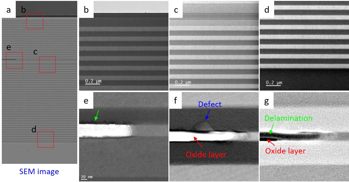
a is a cross-sectional SEM image of the VCSEL.
b-e are STEM images take at locations marked by the red dotted rectangles in a.
f is a STEM image taken from a different VCSEL sample at around oxide layer, where one defect is found.
g is a SEM image taken from another different VCSEL sample, where delamination is found at around oxide layer.
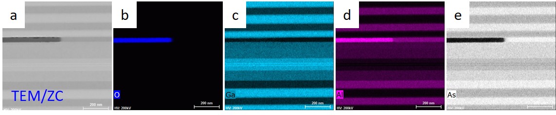
EDS mapping analysis at around the oxide layer of the VCSEL.
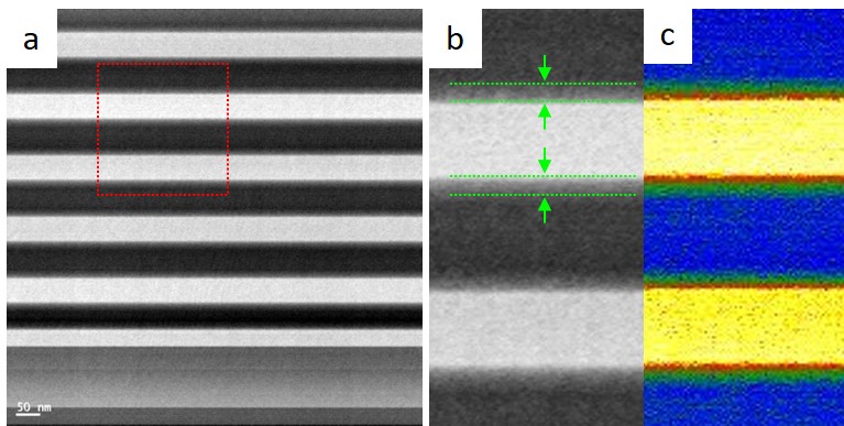
a is a cross-sectional STEM image of the VCSEL multilayer DRB.
b is a zoom-in STEM image from a, marked by the red dotted rectangle.
c is full-color rendering of b.