 TECHNOLOGY INNOVATIONS
Quartz device is a common component in all electronic products from EV, 5G, IoT, aerospace, and AI.
It provides consistent, reliable, and high-performance frequency control (timing).
Due to it’s size up to few millimeters, cross-sectional quartz preparation cannot be easily achieved by Ga FIB.
Such job can be fulfilled by Plasma FIB, PFIB.
Here, we are going to use a state-of-the-art tool, PFIB, to unveil fine structures of the quartz.
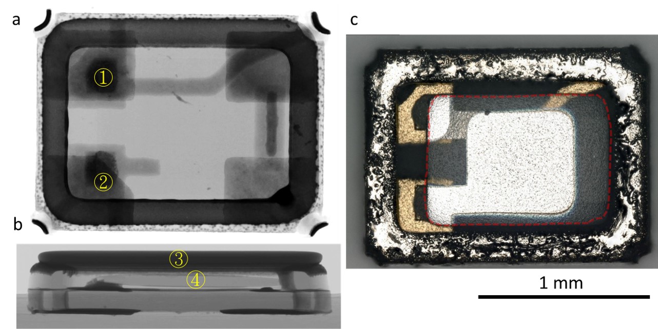
Before PFIB analysis, we start with the non-destructive analysis.
a (PV) & b (cross-sectional) are X-ray image of the quartz device of interest, T240 Ma94.
(1) and (2) are electrodes, (s) is the metal shell, and (4) is quartz.
c is an OM image of the quartz device after decapsulation, where the quartz is marked by the red-dotted rectangle.
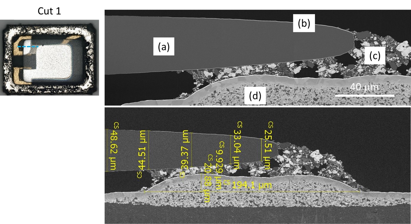
The upper-right image exhibits the PFIB results, where (a) is the quartz itself, (b) is the metal coating above the quartz, (c) is the silver glue, and (d) is the package substrate.
The lower-right image exhibits related dimensions of the quartz.
The cutting location and direction, cut 1, is marked by the sky color-dotted line in the upper-left image.
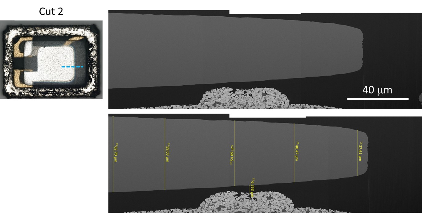
Another cut, cut 2, exhibits the quartz in this location does not attach/glue to the electrode/substrate, the free-standing side.
Related dimensions are also addressed.