Photoresist (PR), a commonly used materials in IC lithography, is extremely sensitive to temperature.
During sample preparation, the sample temperature is normally kept at a higher temperature, above 100 Celsius, in order to have a better conformality of protection layer about photoresists.
The structure of photoresist, however, will have a great possibility been altered or damaged and its pristine structure cannot be observed.
MSS designs a low-temperature ALD to prevent such deformation and damage to deliver precise structural information of photoresists.
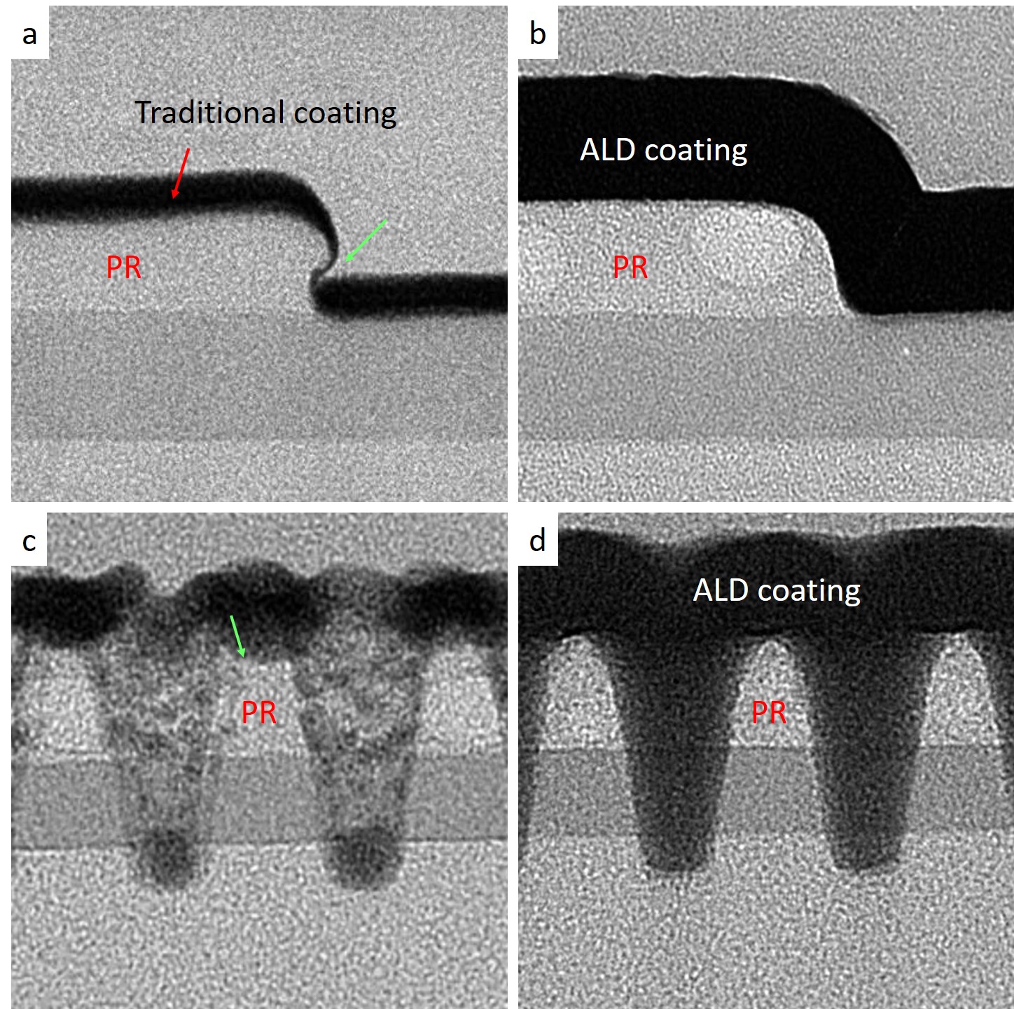
a-d are TEM images of structures of photoresists.
Two different kinds of photoresists are utilized a, b and c, d.
The protection layers in a and c are prepared by the normal coating tool and those in b and d are prepared by MSS low-temperature ALD system.
In a and c, obviously, the structures of photoresists are damaged or altered by comparing with those in b and c, see the areas marked by the green arrows.

Besides providing non-damage TEM analysis, MSS can also deliver high resolution non-coating SEM analysis on photoresists to clearly show prinstin appearances of photoresists.
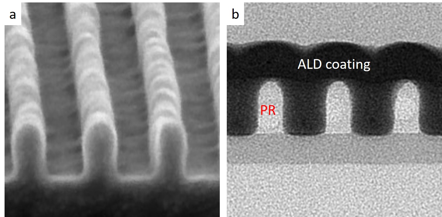
a is a tilted high resolution non-coating SEM image of the photoresist.
For comparison, a TEM image of the photoresist, the same structure as a and the protection layer was prepared by MSS low-temperature ALD coating is shown in b.
By comparing with these two images, obviously, the structures of photoresists stay the same after the low-temperature ALD coating.
 TECHNOLOGY INNOVATIONS