TECHNOLOGY INNOVATIONS
Materials analysis on a VCSEL (Vertical-cavity surface-emitting laser) chip, purchased from the market, OSRAM PLPVCC2 940A_P is carried out.
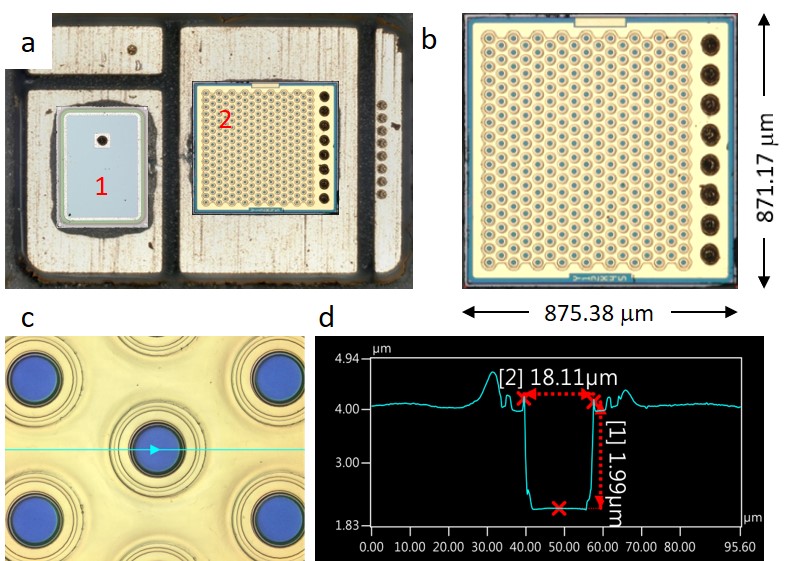
a is an OM image of the VCSEL module after decapsulation, where 1 is power monitor diode and 2 is VCSEL pulsed laser array.
b is an OM image of the VCSEL array chip.
c is topography of the VCSEL acquired by the 3D laser confocal profile.
Cross-sectional profile , d, cross an aperture shown in c (the sky color line) exhibits diameter and depth of the aperture.
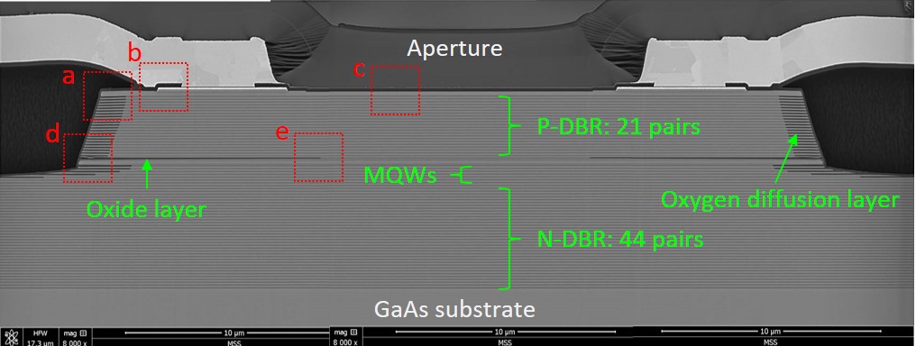
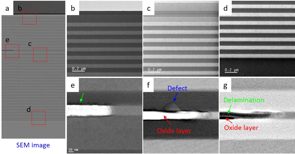
Cross-sectional overview SEM image of the VCSEL of interest, where the inner structures are addressed.
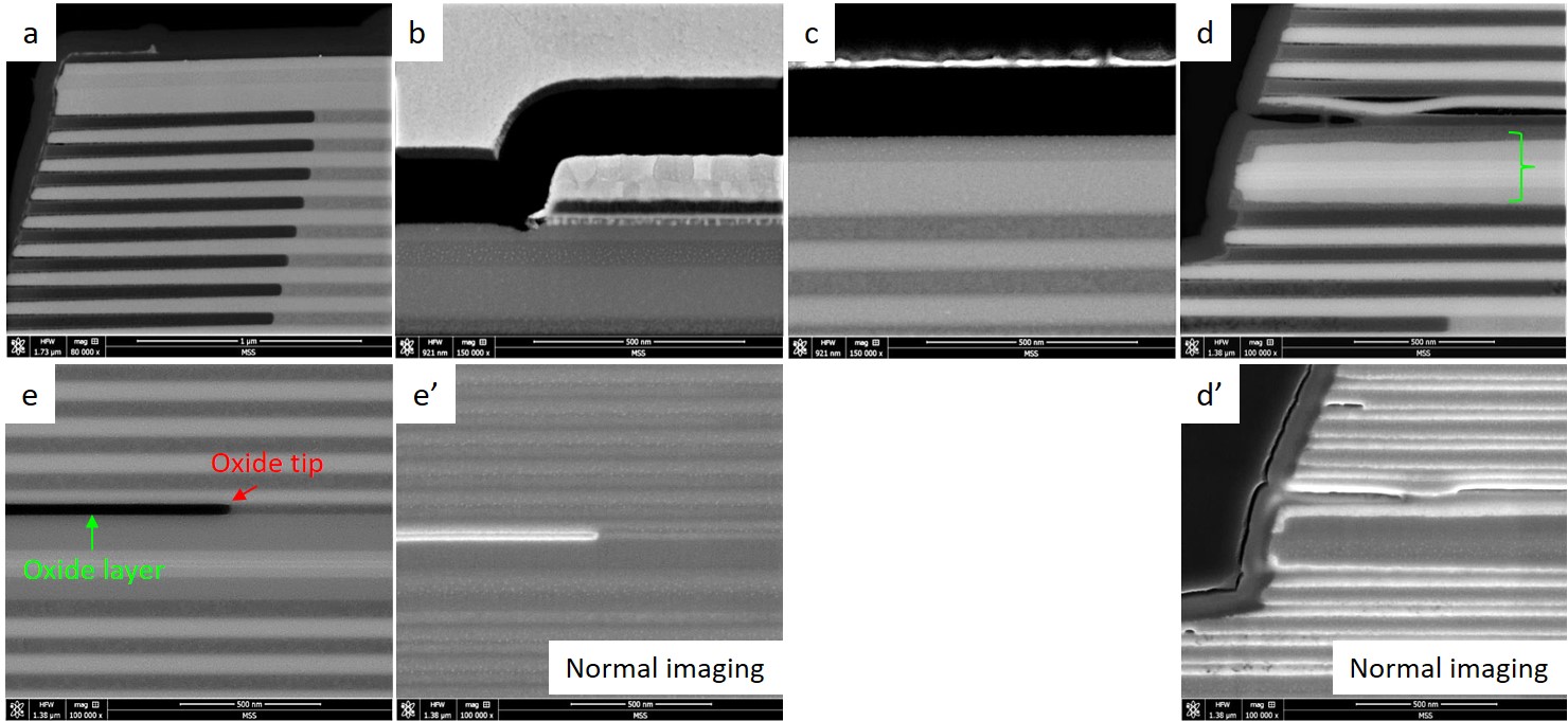
a-e are cross-sectional SEM images of the VCSEL taken at the areas marked in the previous image by the red rotted rectangles.
These images are acquired with MSS advanced imaging method, where fine structures can be clearly observed.
For comparison, d’ and e’ are SEM images taken at the same areas as d and e but with normal imaging methods.
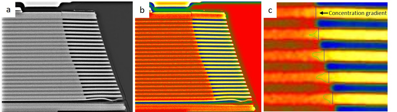
a is a SEM image of the VCSEL acquired by the advanced imaging method.
b is full color rendering of a.
c is a zoom-in image of a, where the concentration gradient profiles can be clearly seen, see green dotted lines.