 TECHNOLOGY INNOVATIONS
NAND flash memory, a type of non-volatile storage memory, can be found everywhere in our daily life, such as USB flash drivers and HD drivers.
The layer of 3D NAND has increased from generation to generation in order to lower the cost-per-bit.
At the same time, processes are more and more challenging .
Therefore, it is interesting to understand its processing details by materials analysis.
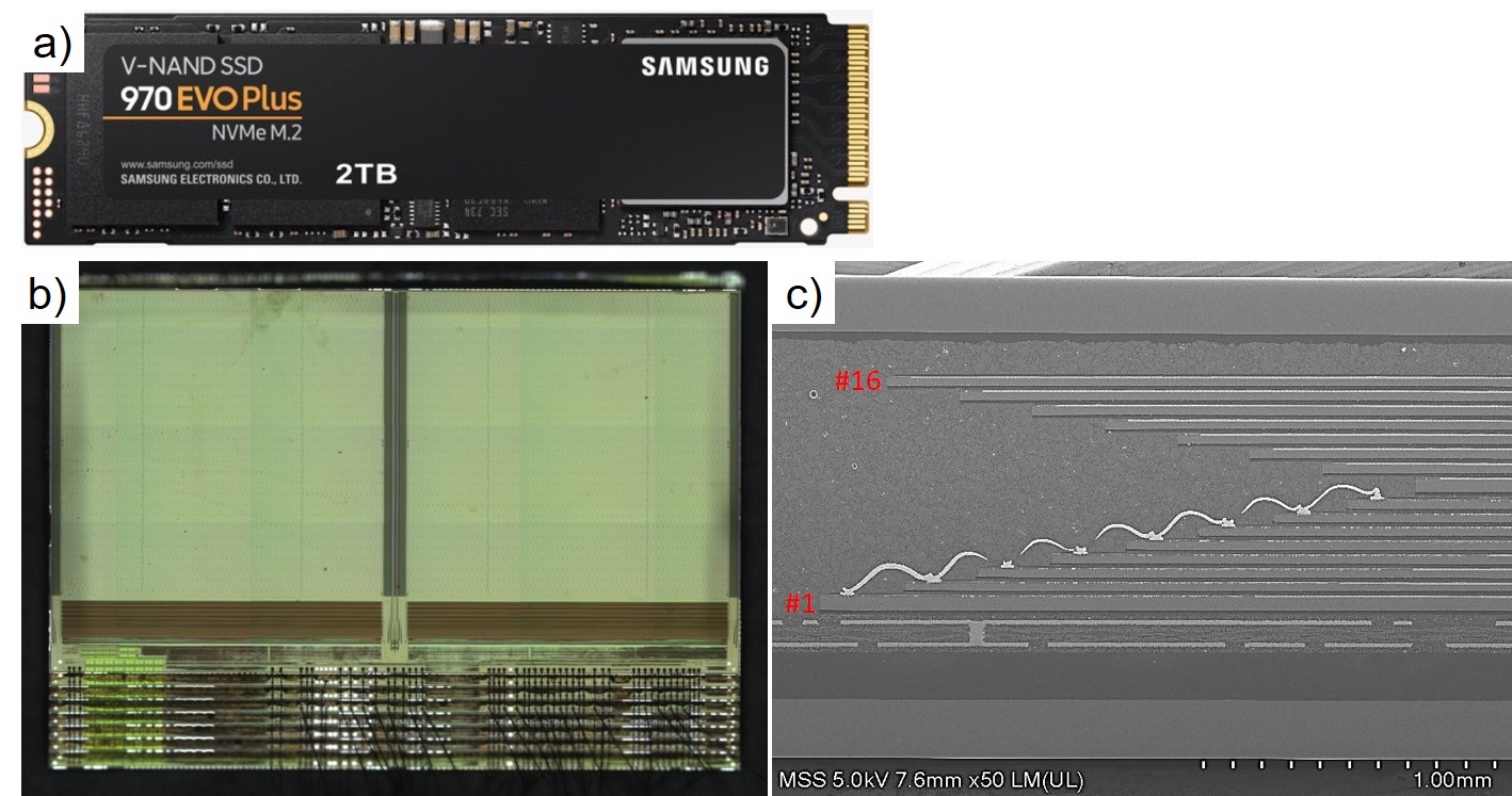
Materials analysis on 3D V-NAND, Samsung V-NAND SSD 970 EVO Plus with a capacity of 2 TB purchased from the market, shown in a, is utilized.
b is an OM image of the Samsung’s 1TB 92-layer 3D V-NAND.
Cross-sectional SEM image of the 92-layer 3D V-NAND dies is shown in c, where dies are stacked in the vertical direction.
Each package includes 16 V-NAND dies (#1 to #16).
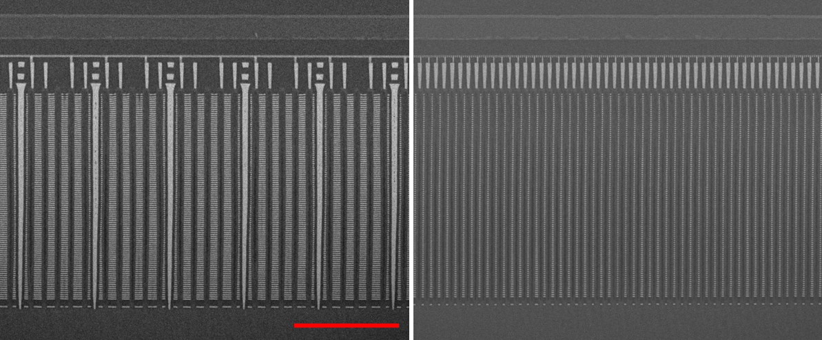
Cross-sectional SEM images, prepared by FIB with MSS niche recipe, in two perpendicular direction (X and Y), of the 92-layer 3D V-NAND cell array.
Severe curtain effects normally observed in big area FIB cuts and strongly affect imaging quality are not found in these images, suggesting MSS FIB recipe can drastically improve such artifacts.
The red scale bar is 2 m.
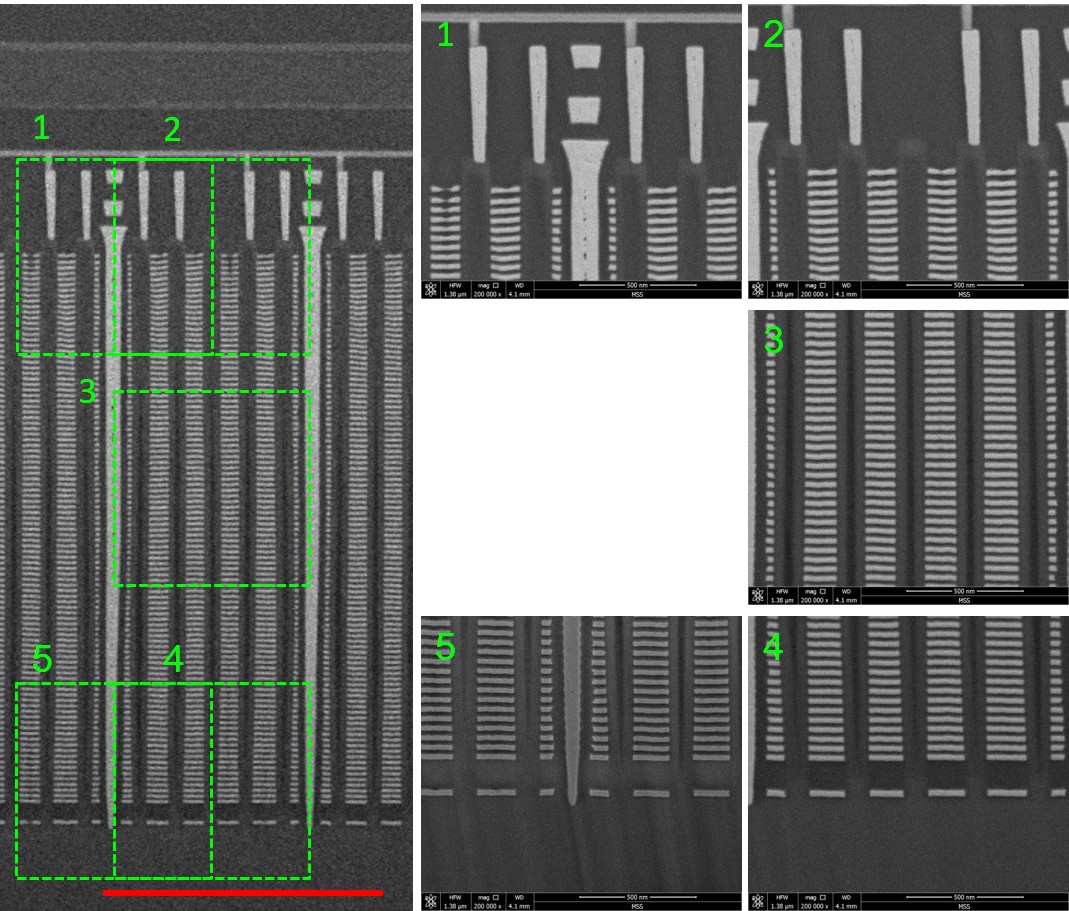
Zoom-in SEM images of the 3D V-NAND in the previous image.
The imaging areas are marked by the green dotted rectangles and numbers.
From 1-5 images, high magnification SEM images of structures of interest at different locations along the 3D V-NAND structure can be clearly obtained.
Curtain effects can only be barely seen.
The red scale bar is 2 m.
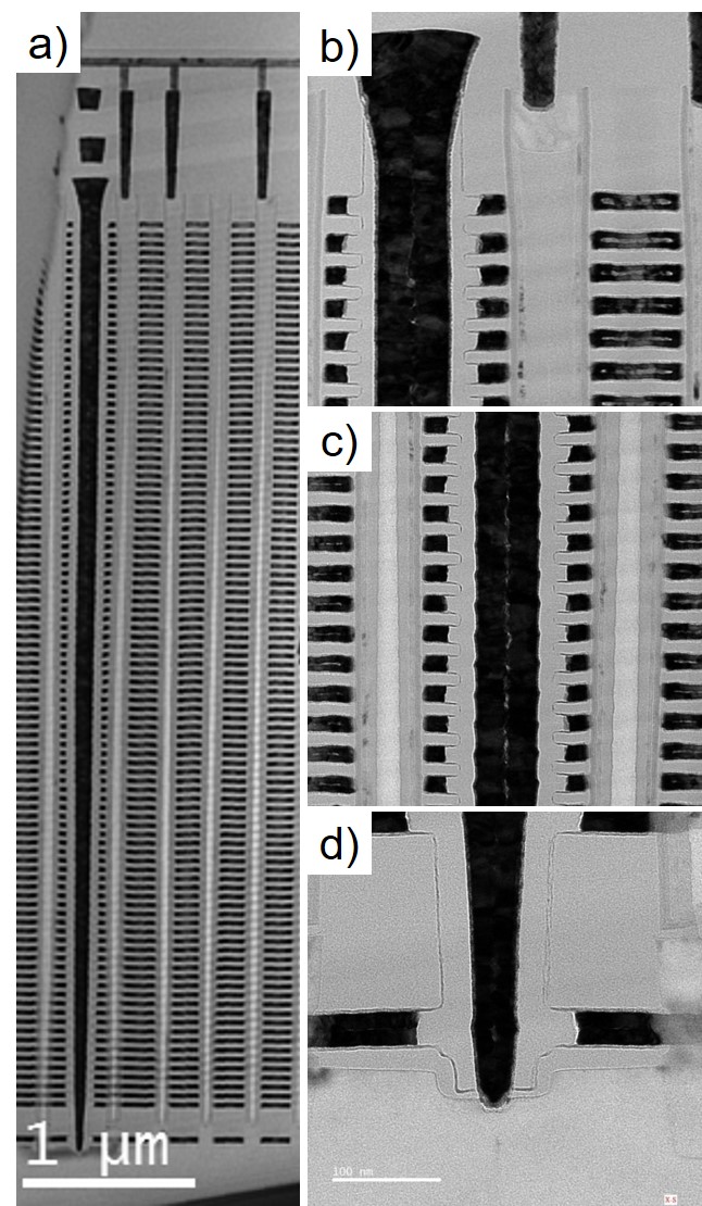
a is a cross-sectional TEM (XTEM) image of the 3D V-NAND floating gate structure.
b-d are zoom-in XTEM images of a taken at upper b, middle c, and bottom d locations.
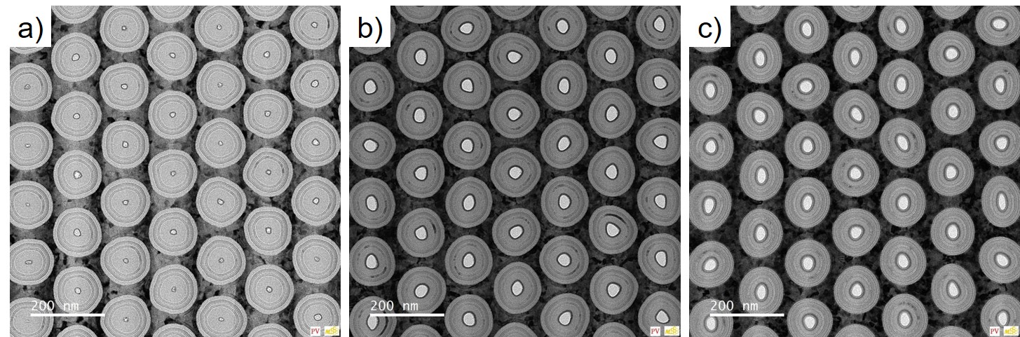
Plane-view TEM images of 3D V-NAND taken at upper a, middle b, and bottom c locations.
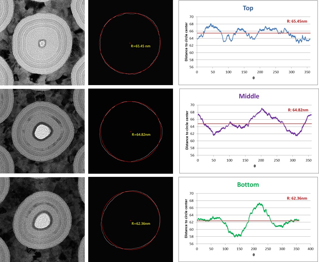
Roundness analysis (MSS algorithm) on the 3D V-NAND doughnut-like structure taken at upper, middle, and bottom locations.
From the results, it clearly shows the diameter of the doughnut-like structure decreases with the depth, as well as the roundness.

Clear elemental distribution of the cell array of the 3D V-NAND can be obtained by TEM/EDS analysis.