 TECHNOLOGY INNOVATIONS
SEM and EDS are commonly-used tools for structural and chemical analyses in IC industry. With the help of the new generation windowless EDS, MSS demonstrates superior quality of SEM and EDS analyses.
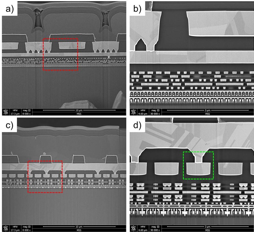
a is a X-cut cross-sectional SEM image of the Samsung Galaxy S8 CPU at the 6T-SRAM area. b is a zoom-in SEM image at an area marked by the red dotted rectangle in a. Y-cut cross-sectional SEM image also at the 6T-SRAM area is shown in c. d is a zoom-in SEM image at an area marked by the red dotted rectangle in c.
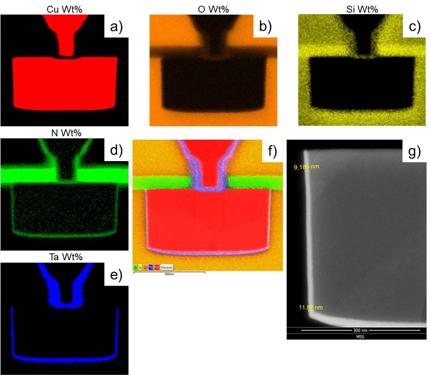
Superior EDS analysis is carried out on an area marked by the green dotted rectangle in d in the previous image. Individual elemental distribution is shown in a Cu, b O, c Si, d N, and e Ta. Overlaying all detected elements is exhibiting in f. g is a zoom-in SEM image at the edge of the Cu wire, showing the thickness of the Ta layer is 9.19 nm (top) and 11.87 nm (bottom). In e, Ta signal can be clearly resolved suggesting that the spatial resolution of MSS EDS can be at least down to 10 nm.
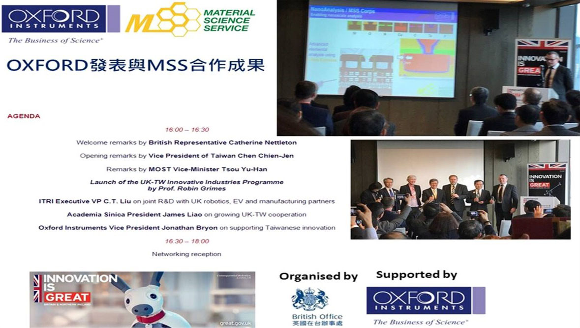
MSS superior SEM and EDS analyses are highly recognized by world-renowned clients and the significant results have been presented in an important activity.