 TECHNOLOGY INNOVATIONS
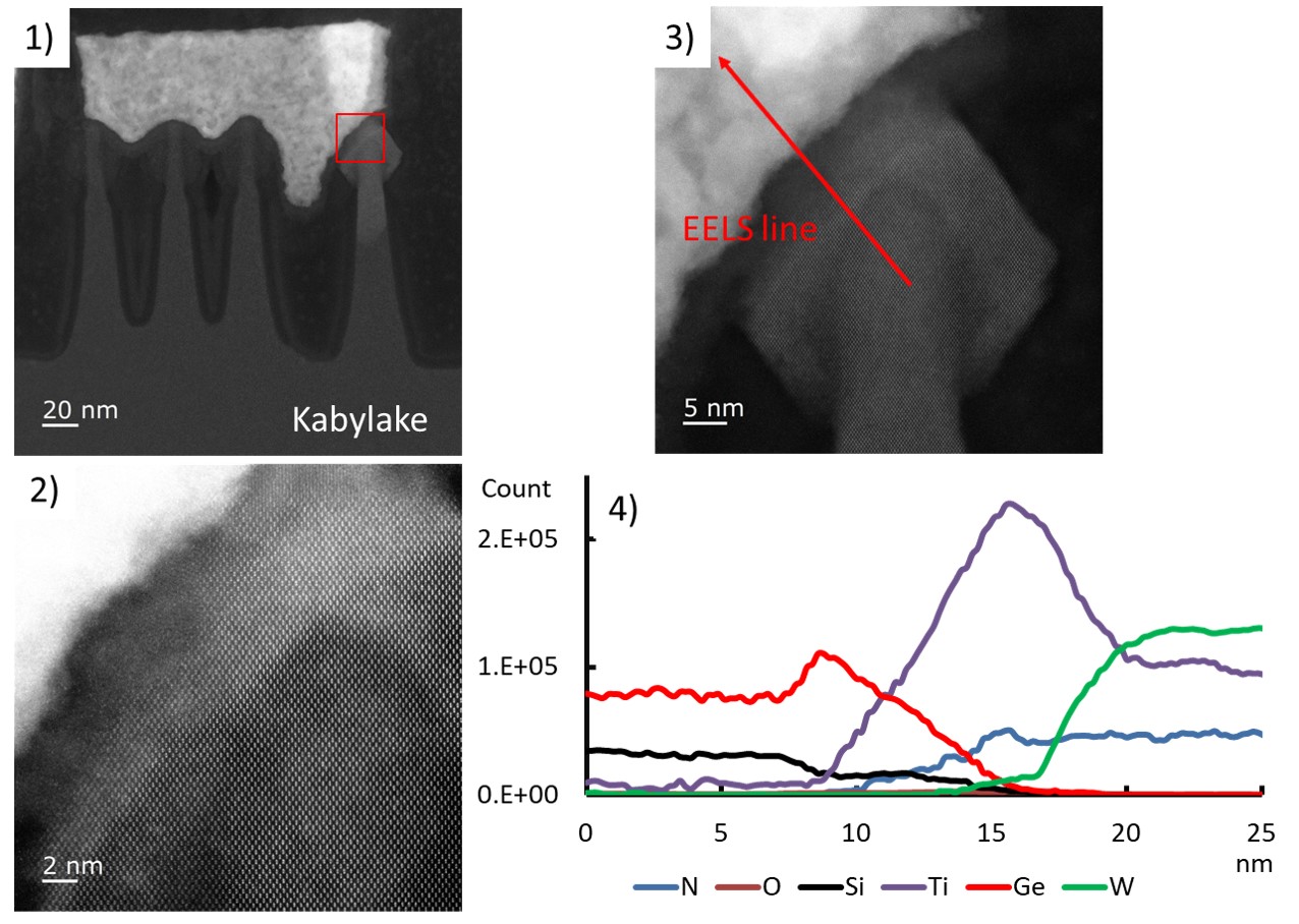
EELS is utilized for chemical analysis mainly for light elements (C/N/O) as well as chemical state determination. MSS provides superior EELS analysis with high spatial resolution.
1) to 3) are STEM/HAADF images of the FinFET structure with different magnifications. The sample is 14 nm plus technology node intel Kabylake chip, purchased from the market. 4) exhibits EELS analysis along the red arrow in 3).
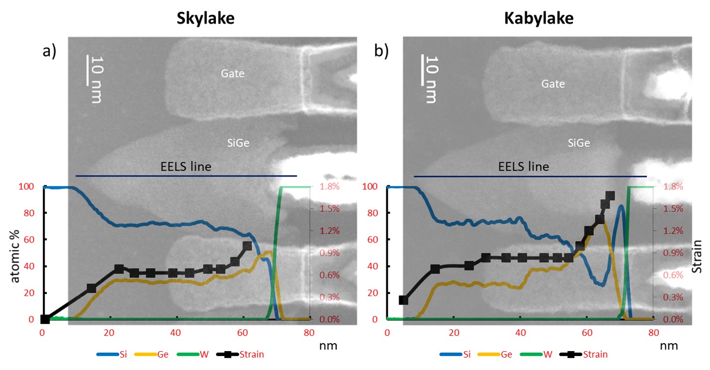
EELS analysis is carried out on a) Skylate chip (14 nm) and b) Kabylake chip (14 nm plus). With the help of the STEM Moiré Analysis, strain inside the SiGe can be obtained (the black curves). Essentially, the strain increases with increasing Ge composition (the yellow curves).
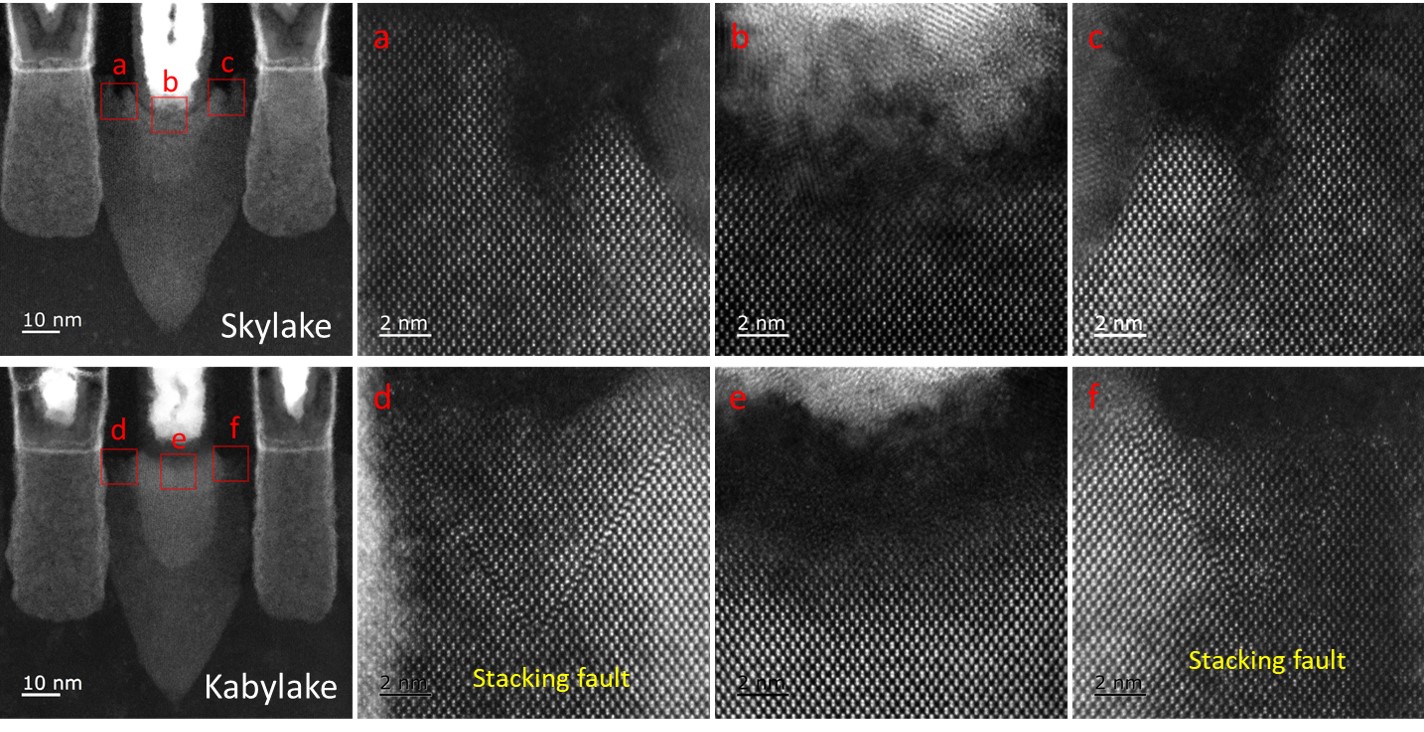
TEM/HAADF images of Skylate and Kabylake chips with different magnifications. Stacking faults, believed to be highly related to the higher Ge composition, can be found at the top of the SiGe structure (d and f) in the Kabylake chip.