 TECHNOLOGY INNOVATIONS
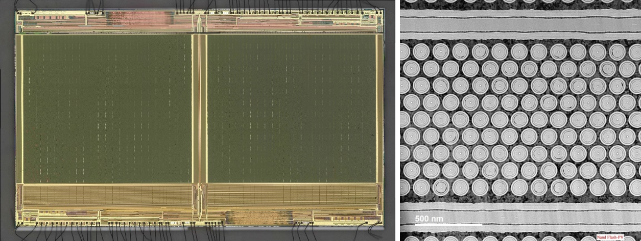
a Optical microscope image of a 128 GB NAND flash memory, b PVTEM image of the vertical channel.
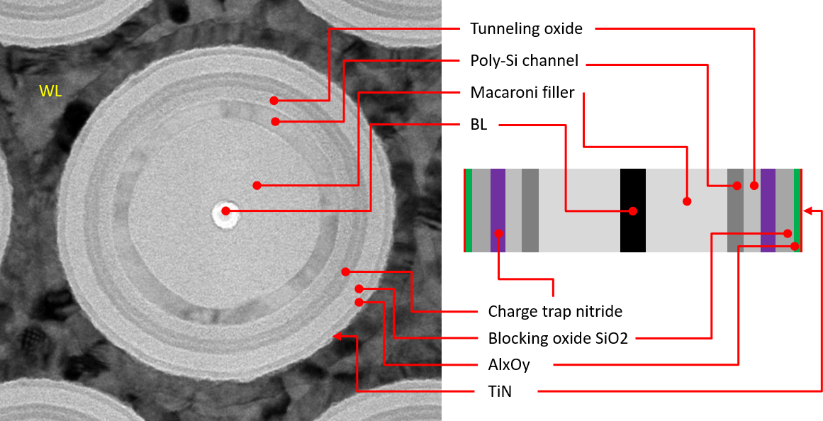
The left side is a PVTEM image of the vertical channel, and the right side is a cartoon showing the structure of each layer of the vertical channel.
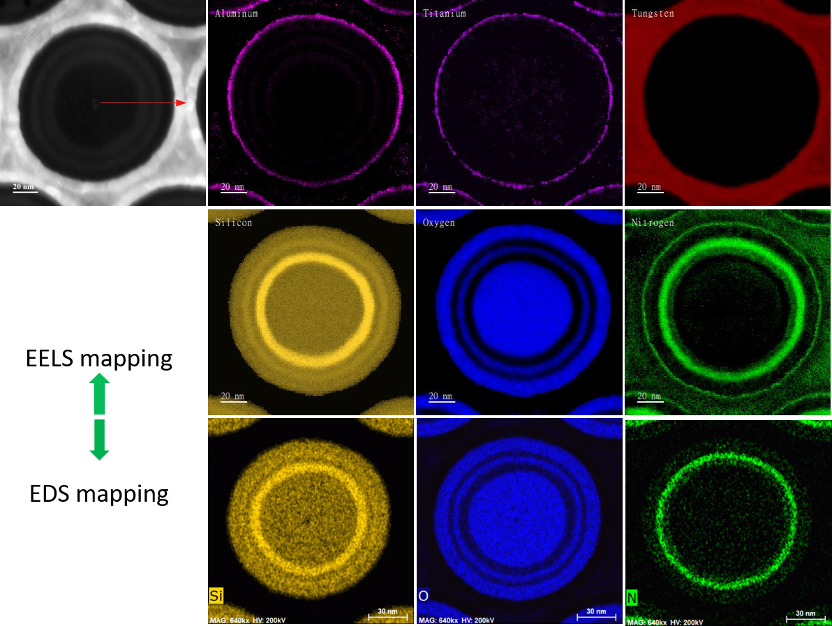
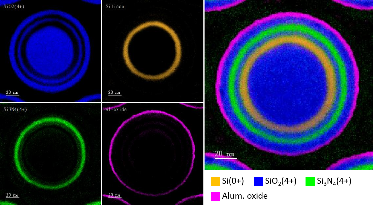
The EELS mappings of the vertical channel are shown in the first two row, and the EDS mappings of three elements Si, O, and N are shown in the third row.
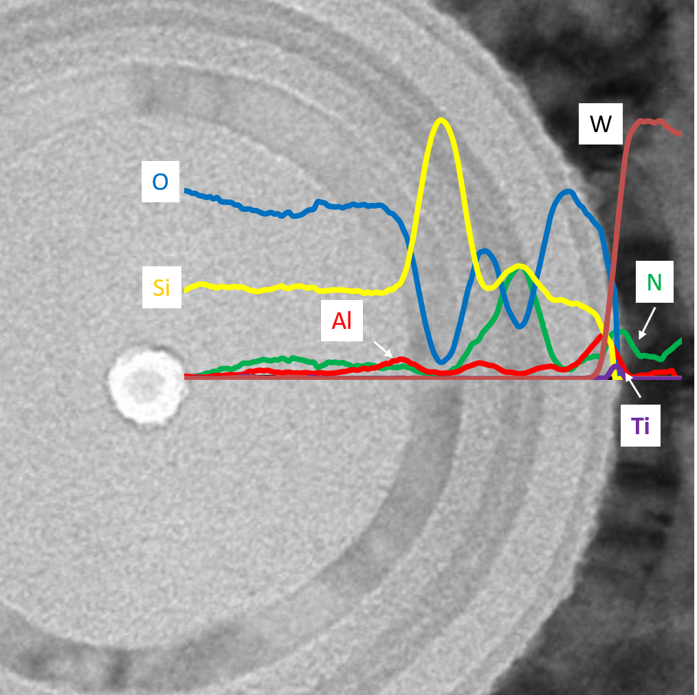
EELS spectrums overlaid with the PVTEM image of the vertical channel.
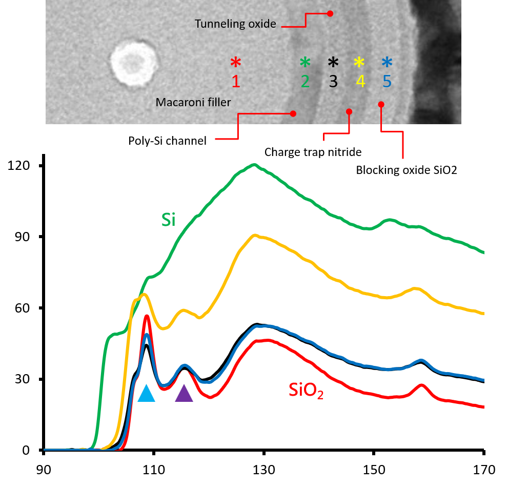
The fine-structure spectrums of ELNES, with the five analysis positions marked in the above image.
The small images on the left are ELNES phase mapping, and the right is the result of superimposing the small images on the left.