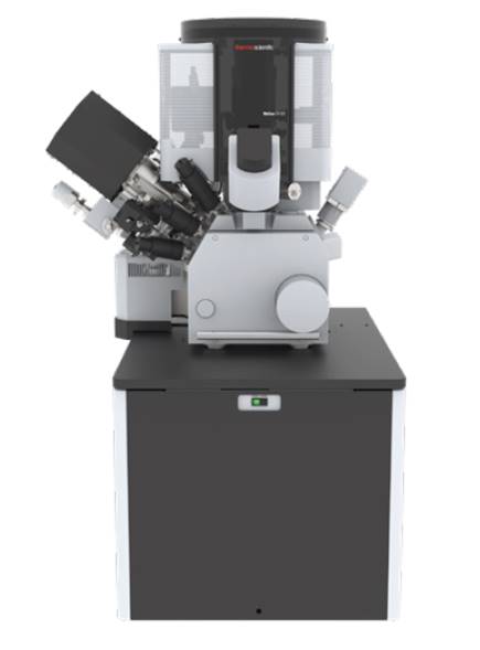
Plasma FIB
▍Plasma Focused Ion Beam - Scanning Electron Microscopes (PFIB) Dual Beam
▍PFIB cut
Small dual beam FIB (Ga ion source), has been widely used for precisely preparing and observing cross-sectional samples of interests, especially in IC industry. Due to the nature of the Ga source, practically, the size of opening window is normally well below 100 um. For preparing bigger structures (few hundreds micrometers in size), such as bumps or 2.5D/3D package, FIB is not recommended.
MSS installed a new generation plasma FIB (PFIB) with Xe+ ion source can extend the opening window up to few micrometers. The milling speed is at least 20X faster than the small DB FIB and with the help of the cutting edge design of the sample holder, sample damage, such as curtain effect, during ion beam polishing can be drastically reduced comparing with the previous GaFIBs.
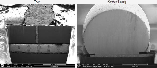
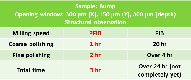
▍Case Study 1
300um × 300um Cross-section (Bump)
.png)
▍Eng. Contact Window
Ms. Chen ext.6211
E-mail: lynn_chen@msscorps.com